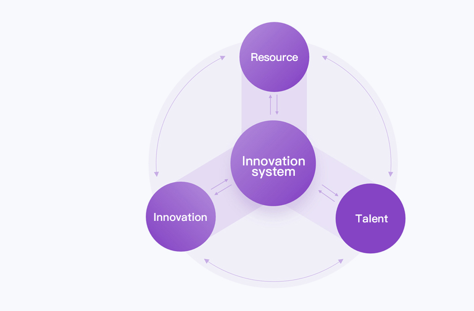
Technology R&D
Technology R&D
Defining the Next Generation of
Micro-LED Display Technology
At the forefront of pixel and optical innovation, INNOSHINE Semiconductor leverages end-to-end technological expertise to transform Micro-LED from a laboratory concept into an accessible future technology.
Driven by the mission of being a core technology innovator, an industrialization catalyst, and a value-ecosystem builder, INNOSHINE Semiconductor has embedded “Technology R&D” into its corporate DNA.
Breaking Through Core Technologies Across the Entire Industrialization Chain
The path toward Micro-LED industrialization is filled with systematic technological barriers spanning materials, chips, and system integration. At the heart of INNOSHINE Semiconductor’s R&D strategy is the precise identification and systematic resolution of these bottlenecks, building fully self-developed technology capabilities from foundational chips to advanced packaging. With a forward-looking strategy, we focus on four core technology domains to establish a self-controlled and fully integrated technology ecosystem:

Breaking the barriers between the laboratory and the factory, transforming cutting-edge technologies into scalable, high-performance, and competitive products, and accelerating the adoption of Micro-LED technology across global markets.
The path to the industrialization of Micro-LED is fraught with systematic technical barriers ranging from materials and chips to integration. The core of Yuexu Semiconductor's R&D strategy is to precisely target and systematically overcome these bottlenecks, building end-to-end independent technological capabilities from foundational chips to advanced packaging. With forward-looking planning, we focus on four key core segments to establish an autonomous and controllable technological loop.

Break down the barriers from laboratory to factory, transforming cutting-edge technology into mass-producible, high-performance, and competitive products, accelerating the global market accessibility of Micro-LED technology.
The path to industrialization of Micro-LED is fraught with systemic technical barriers ranging from materials and chips to integration. The core of Yuanxu Semiconductor's R&D strategy is to precisely focus on and systematically overcome these bottlenecks, building end-to-end self-developed technological capabilities from foundational chips to advanced packaging. With forward-looking planning, we concentrate on four key core segments to establish a self-controlled technological loop.

Break down the barriers from laboratory to factory, transforming cutting-edge technology into mass-producible, high-performance, and competitive products, accelerating the global market accessibility of Micro-LED technology.
Chip Architecture
Design
Chip Thin-Film
Technology
Mass Transfer
Process
Advanced
Packaging
Defining R&D Direction Through End-User Value
True innovation begins with insight into the future. INNOSHINE Semiconductor consistently adheres to a “Scenario-Driven, Value-Oriented” R&D philosophy:

Starting from the ultimate display experience, we work backward to deconstruct technology implementation pathways—translating the unique requirements of commercial displays, professional displays, artistic displays, and emerging display applications into precise technical specifications and development objectives. Through deep collaboration with global partners, we not only provide advanced Micro-LED chips and modules but also focus on delivering customized system solutions, ensuring that every technological breakthrough translates into tangible market competitiveness for our customers.
Exploring Uncharted Territory
Pioneering the Next Generation of Display Technology
While addressing the critical challenges of current industrialization, INNOSHINE Semiconductor has already set its sights on a more distant future. We are actively exploring technological “frontiers,” systematically laying the foundation for next-generation display innovations:

From fundamental exploration of advanced materials, to the development and breakthrough of revolutionary processes, and further to the deep integration of cross-disciplinary technologies—we are committed to building future-oriented technology reserves and ecosystem capabilities. By integrating innovations across materials science, chip design, manufacturing processes, and system applications, we focus not only on technological evolution itself, but also on its transformative impact on display experiences, industry structures, and application scenarios.

With continuous forward-looking R&D as our foundation, INNOSHINE Semiconductor is committed to working alongside global partners to define the future of display technology.
Materials Science Chip Design Manufacturing Processes System Applications
Materials Science
Explore innovations in fundamental materials such as novel wide-bandgap semiconductors, quantum dot luminescence, and high-performance flexible substrates.
Chip Design
Developing revolutionary paths such as single-chip integration, 3D stacking, and selective growth that are expected to simplify the manufacturing process.
Manufacturing Processes
Integrating sensing and computing units with Micro-LED to develop intelligent light-emitting units with sensing and interactive capabilities.
System Applications
Promote the deep transition of display technology from "functional implementation" to "scene empowerment". Through interaction with artificial intelligence, the Internet of Things, flexible electronics, and human-computer interaction. Deep integration of mutual technology, committed to creating the next generation of intelligent display system with "display as life"
Materials Science
Chip Design
Manufacturing Processes
System Applications
A Sustainable Innovation Ecosystem
Building an Integrated R&D Foundation of Talent, Resources, and Mechanisms
Research Team:
Core team members possess an average of more than 10 years of industry experience, combining technological vision with engineering expertise and continuously advancing the frontiers of display technology.
R&D Investment:
40% of annual revenue is invested in R&D, ensuring end-to-end resources from fundamental research to engineering validation, and driving continuous technological iteration and breakthroughs.
Advanced Facilities:
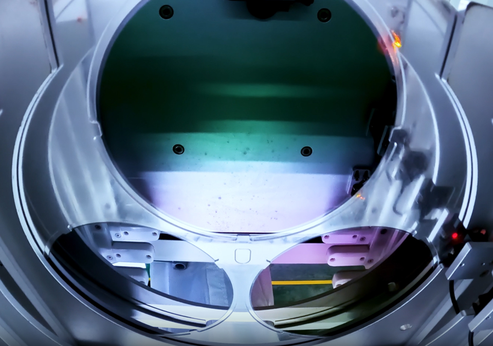
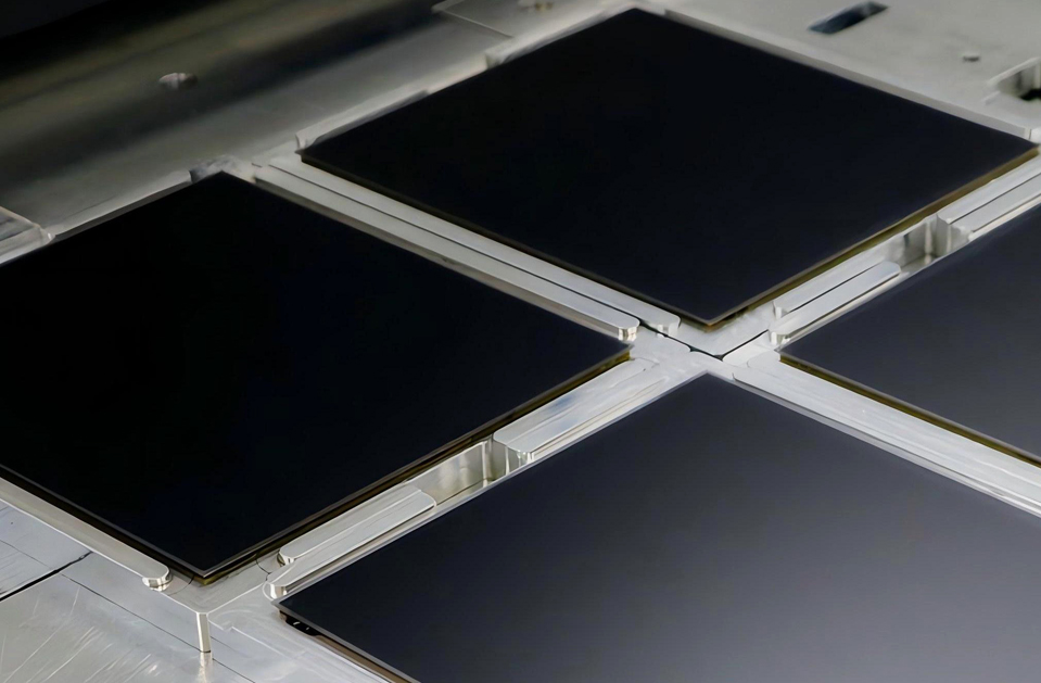
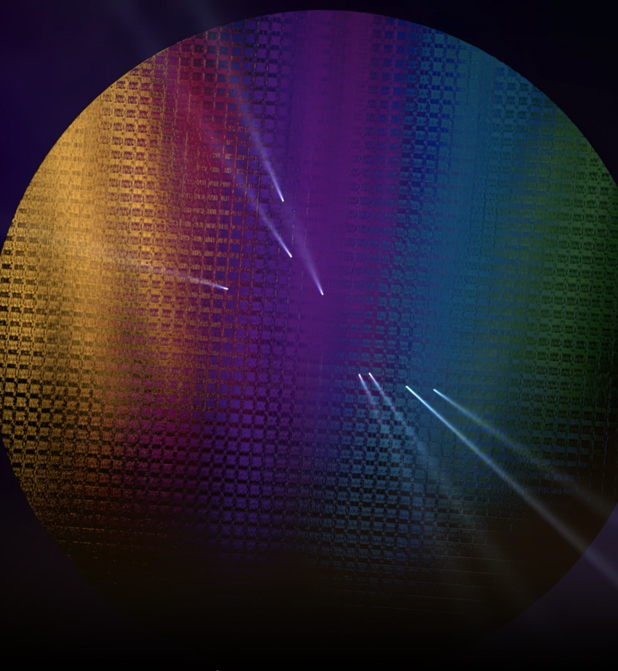
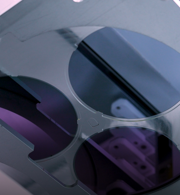
Equipped with Class 1,000 and Class 100 cleanrooms, as well as complete pilot production lines, covering end-to-end development and validation capabilities from materials and chips to modules, providing strong support for technology commercialization.
Efficient Mechanisms:
Implementing cross-functional collaboration and agile development processes to accelerate the transformation of technology into products and respond rapidly to market and customer demands.
>
20
%
R&D headcount
~
300
person
team size
100
+
item
number of patents
Building a Strong Intellectual Property Moat
INNOSHINE Semiconductor has obtained Intellectual Property Management System Certification, successfully establishing a robust intellectual property protection framework. The company has built strong technological advantages in third-generation semiconductor substrates, chips, and heterogeneous integration technologies, securing a leading position in innovation.
100
+
Total Patent Applications Filed
40
Invention Patents
75
Utility Model Patents
10
Trade Secrets and Proprietary Technologies
2
PCT International Patent Applications