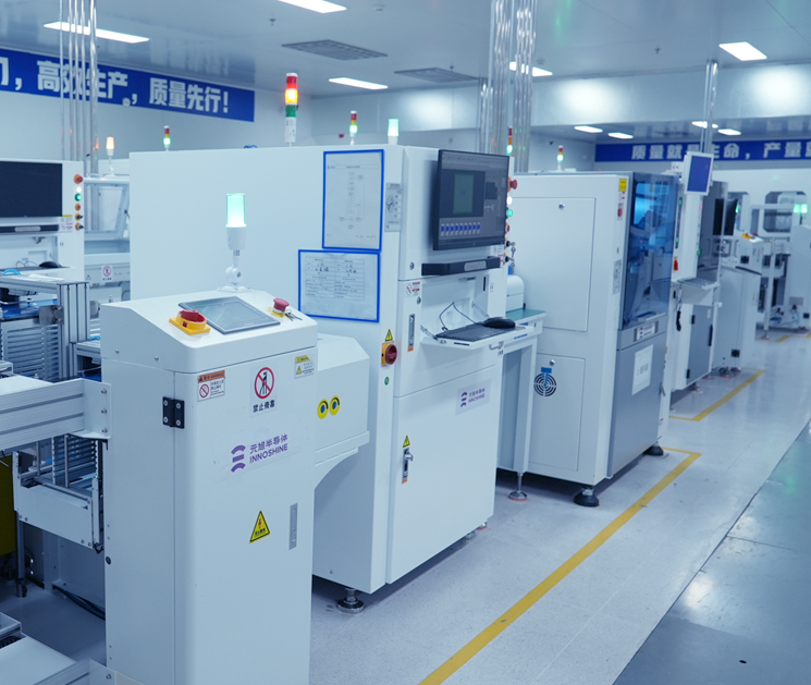
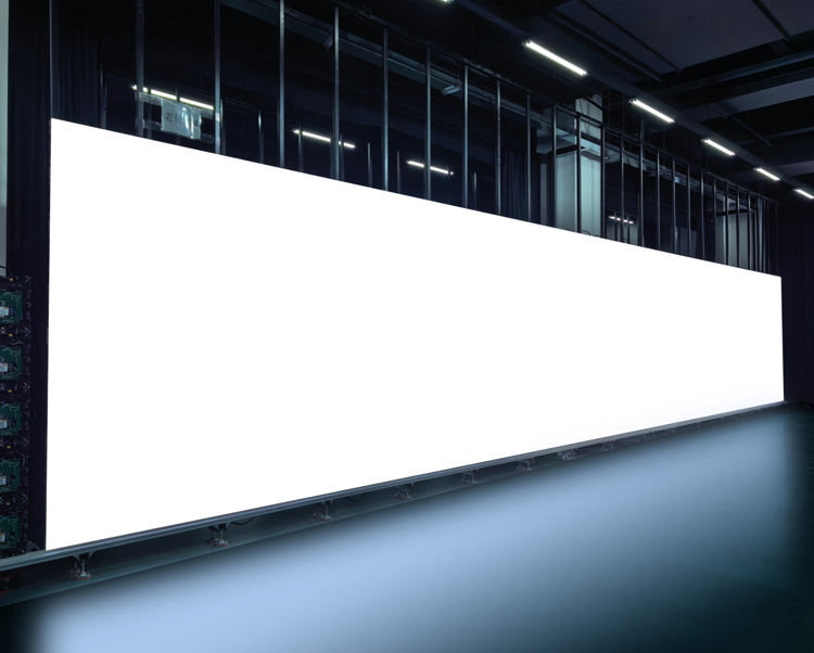
Three-Tier Defect Inspection
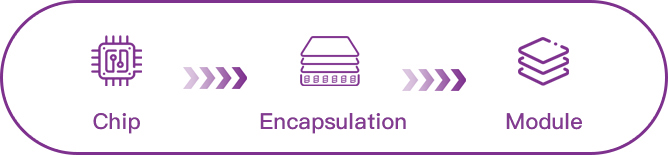
Layer-by-Layer Screening from Chip to Module
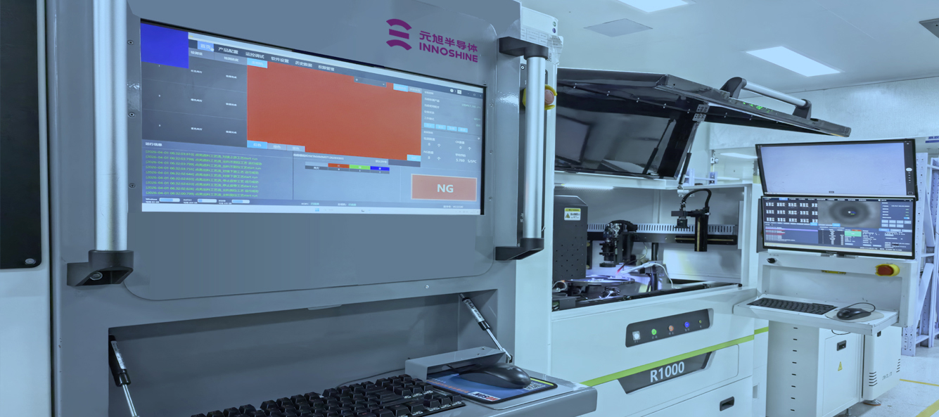
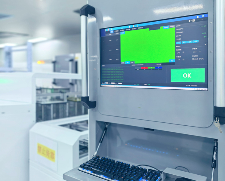
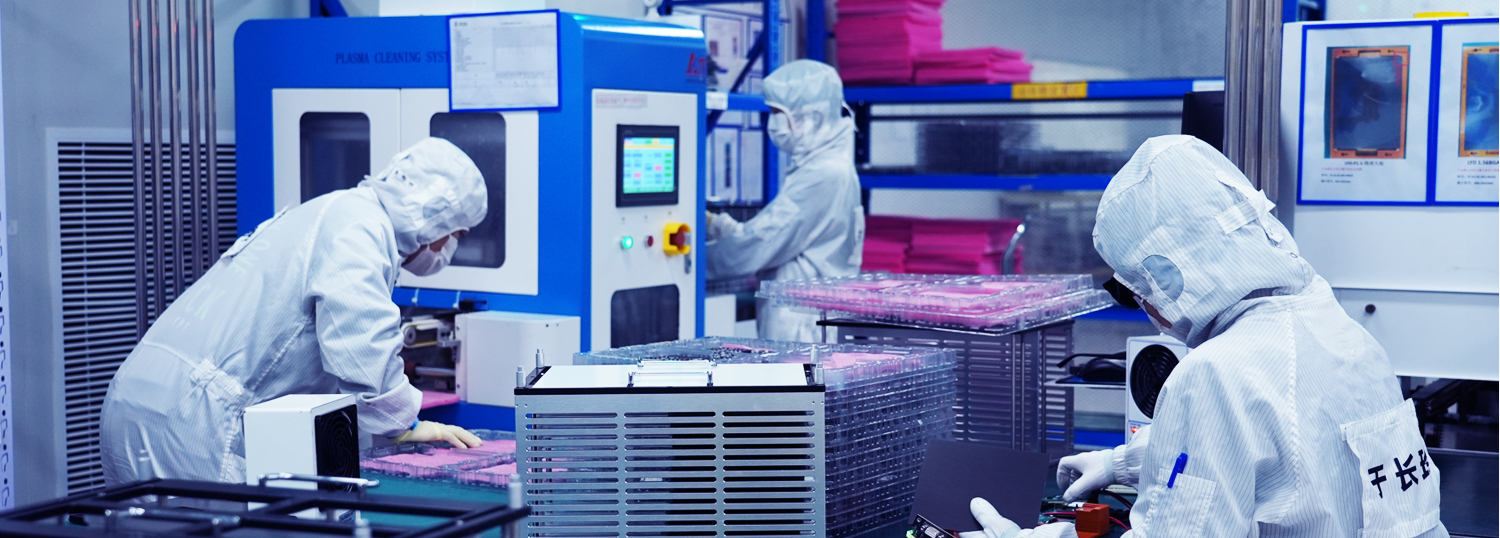
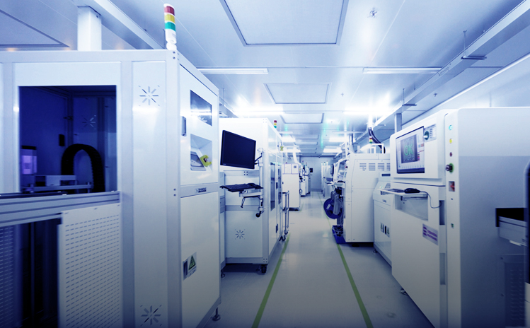
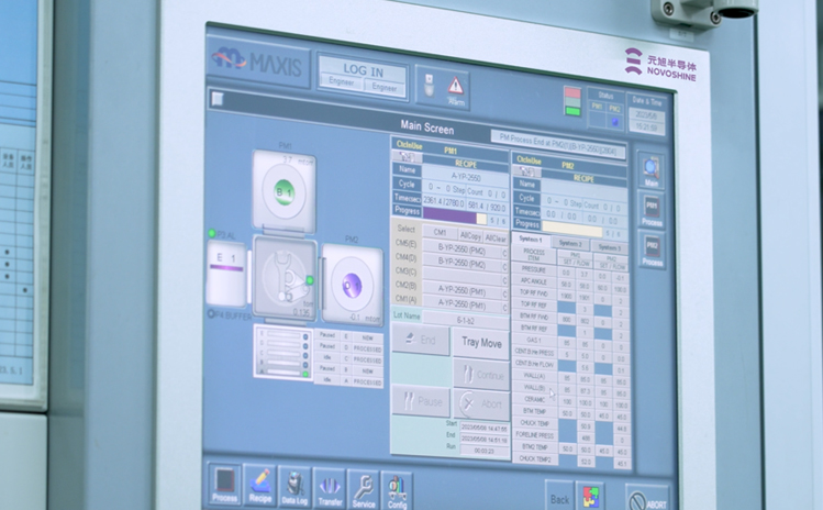
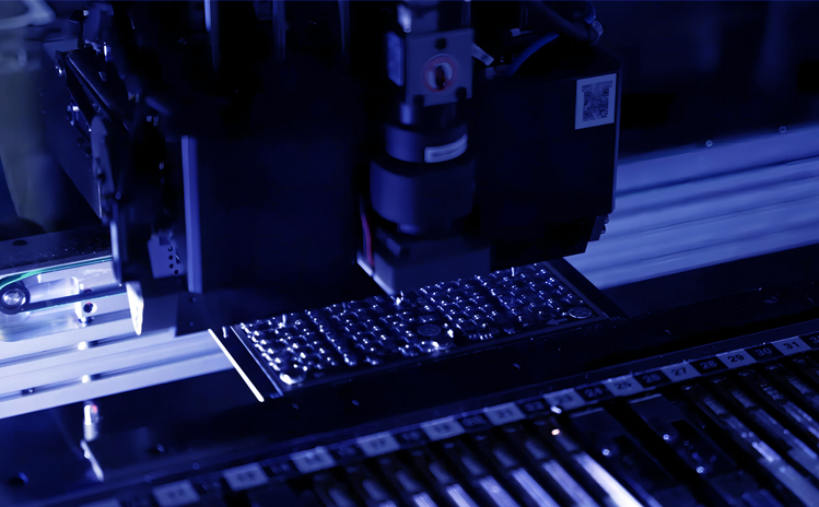
At the wafer and chip stages, two rounds of high-precision AOI visual inspection enable megapixel-level defect detection, intercepting microscopic defects at an early stage; after packaging is completed, full-pixel-array scanning is performed to ensure that every chip meets stringent quality standards before integration. Triple Filtering, Leaving No Place for Defects to Hide.
High precision AOI visual inspection
Pixel level defect recognition
Full pixel array scanning